|
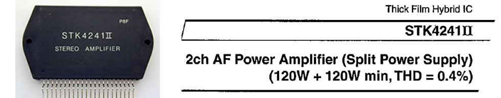
STK4241mk2 The STK series was developed by SANYO sometime in the 90s I believe. They called it “Thick Film Hybrid IC”. Basically, they miniaturized the entire power amplifier into a compact flat pack. This has an advantage in manufacturing as very few components are needed to get it working. It’s a shame Sanyo has stopped manufacturing these STK ICs as they make wonderful projects for diy. Take this STK4241mk2 for example. It’s kind of idiot proof. Great for beginners. And we are looking at 2 channels of 120W each. You won’t need an oscilloscope, signal generator, etc. Just a good soldering iron. Inside the STK4241mk2
Though it’s easy to build a high power amplifier with this STK4241mk2, it’s a golden opportunity to gain some knowledge on the intricacies of how a power amplifier works. The simplified schematic above (Fig 1) will serve as a template. Let’s begin with the signal entering the amplifier. That will be PIN 3 which is the base of TR1. This transistor, together with TR2, form what is called an input differential. The signal then enters the base of TR4, which is the 2nd stage. This is commonly known as the Voltage Amplifier Stage (VAS). From here on, the in-coming signal should have it’s voltage suitably amplified before injecting into the last stage. It is also at this stage that we have the Darlington thermal controller (TR5). This transistor prevents the amplifier from destroying itself when the power transistors heat up. They have a big word for this. It’s called “Thermal Runaway”. TR7 and TR9 are the power transistors in this last current stage. There’s no voltage amplification here. The job is to supply current. Notice TR7 and TR9 are both NPN transistors. This arrangement is known as Quasi-Complementary as opposed to Full Complementary, which uses NPN and PNP. Making it work
Fig 2 shows how easy it is to build a power amplifier of 120W + 120W. All that’s needed are a few passive components like resistors and capacitors. Not one transistor in sight. Try building a discrete amp of this power and chances are you’ll blow it up if you don’t have enough experience. With this STK4241mk2, you can’t go wrong. Starting at PIN 3 again, we can see there’s a high and low pass network. This sets the upper and lower limits of the in-coming signal. PIN 4 is the inverting input. This is where the negative feedback is fed back to. An interesting feature of this amplifier is at PIN 7. This design does not use a current source in the VAS. Instead the VAS is bootstrapped to the output by two 4.7K resistors and the 47uF capacitor. With these two resistors, I can actually fine-tune the idle current in the VAS by changing their values. Apart from the bootstrap technique, the 0.22 ohm resistor at the output is quite unusual. Notice that negative feedback is taken after this resistor, which is between the resistor and the speaker. It got me puzzled for a while. It was only later that I realized that this is current feedback. With this resistor, the global negative feedback is not purely voltage but a mixture of voltage and current. This is rarely seen in power amplifiers. Considering that this is a STK flat pack, I honestly didn’t expect it to have such nice features. It’ll be interesting to see how it performs when the pcbs’ are delivered. Compact PCB
Fig 3 is the pcb for the STK4241mk2. It measures only 4″ X 2-1/2″. On it, you have a complete 2-channel power amplifier of 120W per channel. Pretty incredible. The pcbs are in the process of being manufactured now. I should receive them in 2 to 3 weeks. Once they are delivered, I will bench test them for power output and stability. |
February 20, 2022Amplifiers, Projects
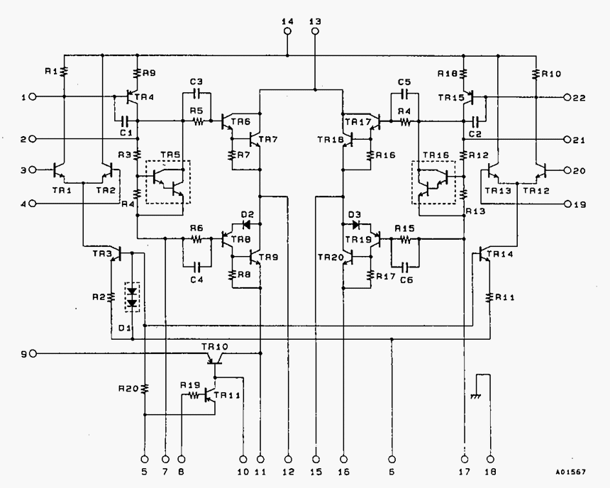
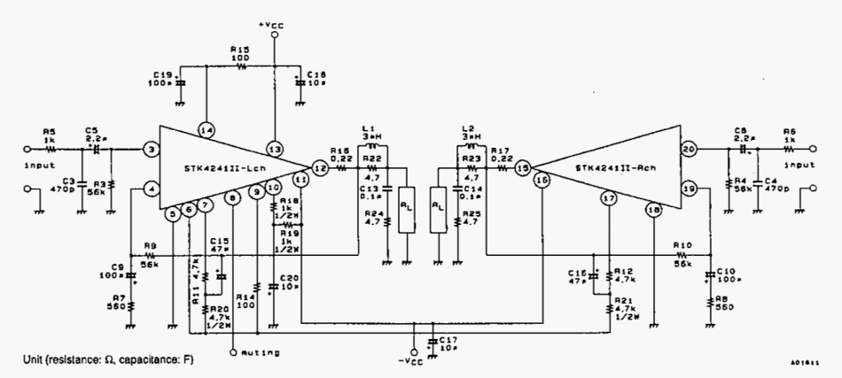 Fig 2 – Circuit of STK4241mk2
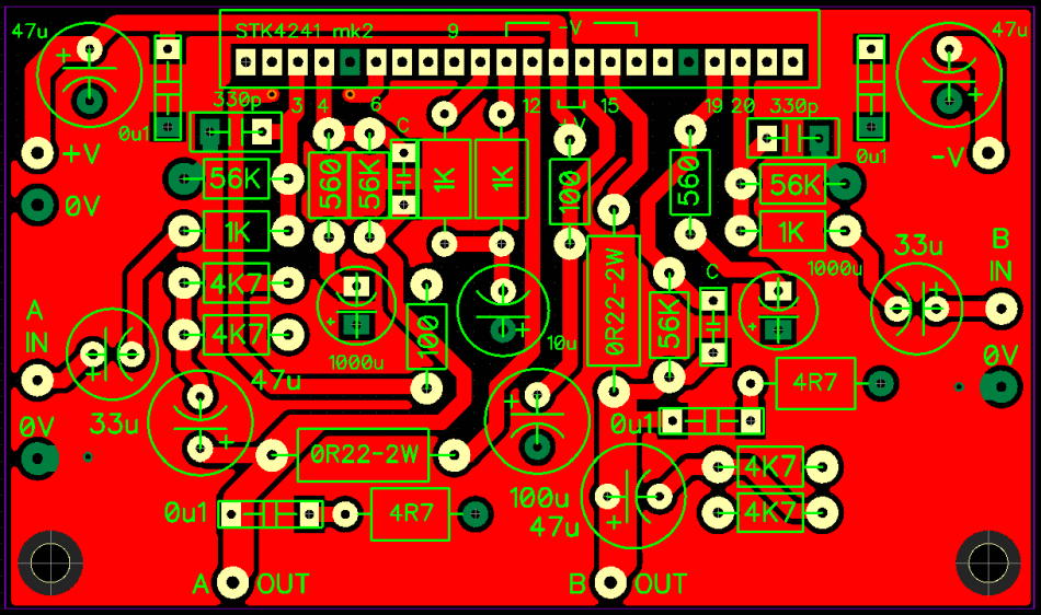 Fig 3 – STK4241mk2 pcb